Materials in Physics
Magnets.
In a ferromagnetic material, magnetic domains are regions where the magnetic moments of atoms are aligned in the same direction. Domain walls are the boundaries between adjacent domains where the magnetic orientation changes. In some cases, these domain walls can act as barriers to the flow of electrons, contributing to electrical resistance.
The 3 primary types of magnets are:
-Ferrite magnets (ceramic magnets): made from a ceramic compound of iron oxide (Fe2O3) with other elements such as strontium, barium, or lead. Ferrite magnets are relatively inexpensive and are often used in various applications.
-Alnico magnets: composed of aluminum, nickel, and cobalt, along with iron and small amounts of other elements. Alnico magnets are known for their strong magnetic fields and temperature stability.
-Neodymium magnets: a type of rare-earth magnet and are the most powerful permanent magnets available commercially. They are made from an alloy of neodymium, iron, and boron (NdFeB), and are widely used in applications where strong magnetic fields are required.
There are also other types of magnets, such as samarium-cobalt magnets, which are another type of rare-earth magnet.
Alnico magnets were historically widely used before the development of neodymium magnets.
The world's strongest magnet, as of 2023, is at the National High Magnetic Field Laboratory in Tallahassee, Florida, where they held the Guinness world record for the strongest continuous magnetic field since 2000. The Earth's magnetic field is .00005 Tesla, a fridge magnet, .01 Tesla, MRI machines up to 3 Tesla, but this electromagnet is at 45 Tesla (11.5 T for a outer superconducting electromagnet and a 33.5 T for an inner resistive electromagnet made of ordinary wire). The coils for the superconducting magnets are made of NbTi and Nb3Sn. The magnet has to be turned on, taking 47,000 amps at 500 volts, taking an hour and a half.
Making high-field magnets with ordinary resistive wire is challenging, with the highest magnetic field limited to only 2 Tesla, with the reason being it's hard to get the heat out of the innermost windings.
Semiconductors.
Part 1 - mobile industry.
In late 2022, Intel controls about 70% of the CPU market, Nvidia about 87% of the GPU market, and AMD 83% of the gaming console processors. Intel makes a lot of 10 and 14 nm server chips used in CPUs, and GPUs in data centers, as well as 28 to 40 nm chips for the auto industry, such as anti-lock brakes and air bags. 5 nm chips, are curretly only made by Samsung and TSMC as of 2022, for AI, iPhones, and other advanced data processing. AMD chips are in Tesla models S and X. Apple parted away with Samsung for their chips for iPhones in 2013, parted away with Intel for their chips in Macs by 2020.
To make 5 nm chips, semiconductor companies use extreme UV lithography machines, that uses small rays of light to etch designs on chips (EUV for extreme ultraviolet lithography). As of late 2021, only 1 company makes these machines, ASML, and these machines cost around $180 million. In 2019, TSMC made up 40% of ASML's sales, so TSMC's customers (AMD and Nvidia) gained the advantage of EUV. Intel 1st produced chips with EUV in 2022, which is 3 years behind TSMC. Intel has plans for a 18-Angstrom chip, for 2025. ASML's previous machines that used deep-UV, were 193 nm wavelength of light, whereas the extreme-UV are at 13.5 nm. DUV chips are used for simpler processors such as toasters, refrigerators, and some electronics in cars. The iPhone 13 is in EUV. For all of ASML's lithography machines sold in 2021, 267 of the 309 sold, were for DUV. Nikon and Canon also make DUV.
EUV light is made from molten tin being shot out at 4,000 psi pressure. The tin is streamed through a calibrated nozzle at a rate of 50,000 droplets per second. A 20 kW CO2 laser hits each droplet twice per second, vaporizing them into plasma. These tiny explosions are what emit the EUV photons. A huge number of tin explosions need to happen because only 5% of photons reach the actual wafer. This has to be done in a vacuum, because air will absorb the EUV photons. As late as 2018, the Trump administration has pressured ASML not to sell EUV machines to China, and that has not happened as of March 2022. There are national security risks on whether ASML shoould still continue to sell DUV machines to China.
1 scientific difference between AMD and TSMC, is silicon on insulator, which is a huge differentiation when it comes to power. TSMC does not use that, AMD does.
Apple used to use semiconductors made by Intel, then Apple debuted its own semiconductors in iPhones in 2010. As of June 2023, all new Mac computers are powered by Apple's own silicon too, ending a 15+ year reliance on Intel. But all of its most advanced silicon is manufactured by Taiwan Semiconductor Manufacturing Co.
Apple launched the 1st iPhone in June 2007, with a 90 nm processor made by Samsung, then in 2008, Apple hired Johnny Srouji, who had stints at IBM and Intel, with the purpose of building their own silicon for the iPhone. The team was about 40-50 engineers. 1 month later, Apple bought 150-person chip startup PA Semiconductor for $278 million. 2 years later, Apple launched their 1st custom chip, the A4, in the original iPad and iPhone 4. They built the "unified memory architecture" that is scalable across products, starting with the iPhone, then scaled to the iPad, then to the watch, and eventually to the Mac. Now, Apple has thousands of engineers working in chip labs, in places like the USA (Austin, San Diego, and Silicon Valley), Israel, Germany, Austria, the UK, and Japan.
In 2019, Apple's chip architect Gerard Williams left suddenly to lead a data center chip startup called Nuvia, where he brought some Apple engineers with him. Apple sued Williams over IP concerns, then Qualcomm bought Nuvia in 2021 for $1.4 billion, in a move to compete in ARM-based processors like Apple's. Then ARM sued Qualcomm in 2022, saying it only licensed their architecture to Nuvia, and not Nuvie's new owner. Apple dropped the lawsuit against Gerard Williams in 2023.
Apple turned away from using Intel's PC processors in 2020, switching to its own M1 chip inside the MacBook Air and other Macs. Intel processors are based on x86 architecture, the traditional choice for PC makers, but Apple based its processors on the rival ARM architecture, which is known for less power and therefore helping batteries last longer. In Sept. 2023, Apple signed a deal with ARM.
Apple doesn't make their own modems yet, Apple uses Qualcomm for its modems, but that relationship was strained following a 2-year legal battle over IP. A settlement brought an end to all legal action in 2019, and then Apple bought the majority of Intel's 5G modem business for $1 billion in a move to develop its own cellular modem. The latter hasn't happened yet, so in Sept. 2023, Apple signed on with Qualcomm to supply its modems through at least 2026.
Global smartphone sales rebound in Oct. 2023 after declining for more than 2 years. Smartphone sales in 2022 were the lowest since 2013.
AI chips: Google has deisnged a tensor processing unit for AI since 2016. Amazon Web Services has had its own AI chips for their data center since 2018, and in Nov. 2023, Microsoft has a new custom AI chip, that could compete with Nvidia.
In 2018, AMD turned to TSMC to make all of its chips, as chip making got expensive, giving AMD far less expenses. In Feb. 2022, AMD discontinued FPGAs (Field-programmable gate arrays).
Part 2 - automobile industry.
Volkswagen was the 1st to use performance chips in their vehicles in 1968, which had computer-controlled electronic fuel injection (EFI).
In 1970, the Air Pollution Control Law (the so-called Muskie Act) was enacted in the U.S., and automobile manufacturers began to promote the development of electronic engine control technology to cope with this situation.
The 1st mass-produced car with computer-controlled electronic fuel injection (EFI) is often credited to the 1975 Chevrolet Cosworth Vega. The Cosworth Vega featured a Bosch electronic fuel injection system called Bosch L-Jetronic. This system utilized an electronic control unit (ECU) to monitor engine parameters and adjust fuel injection accordingly.
In 1974, Toshiba made the 1st chips that Ford used in engine control modules (ECMs), the TLCS-12. Electronics had been used in fuel injection systems since 1968, but these were single components rather than digital ICs (integrated circuits).
In 1976, General Motors announced its partnership with Motorola Semiconductors. Motorola 6802 microprocessor was the 1st chip used in latest 1970s GM cars. It was 8-bit and an off-the-shelf chip adapted for automotive use. In 1978, it was used in Cadillac's Seville models. Not the 1st, but GM (Kokomo Delco plant) used to have its own fab plant, which ran from 1953 till 1991.
(Note: at the time, both Toshiba and Motorola made semiconductors, but only Motorola also made microcontrollers and microprocessors.).
A few years later, General Motors partnered with Delco Electronics for custom ICs and electronic modules, for various applications such as engine control, climate control, and anti-lock braking systems.
In 1983, Ford started a partnership with their 2nd company, Intel, to build ECUs (engine control unit) using custom Intel 8061 microcontroller chips, which was used in most Ford automobiles from 1983 to 1994. During the late 1980s, GM and Chrysler ECMs (electronic control module) would both begin using the 16-bit Motorola 68HC11 microcontroller chip in their vehicles.
In 1994, in a last attempt to save the slowing EEC (electronic engine control) IV microcontroller, Ford used 2 Intel 8065 16-bit chips inside the controller. Shortly thereafter, Ford would be ready to end their long use of Intel micro-controllers and transition to using Motorola's new 32-bit PTEC controllers (powertrain electronics controller). In 2005, Intel announced they were discontinuing production of all automotive versions of their microcontroller chips.
The average vehicle today has anywhere between 50 and 150 chips. Electric cars, however, are total outliers, as they can contain up to 3,000 chips.
Part 3 - video game industry.
The semiconductor for the NES is made from NMOS technology (n-type metal oxide semiconductor), and CMOS (complementary metal oxide semiconductor) for the Super Nintendo and Nintendo64, made by Ricoh for the NES and Super Nintendo, and made by NEC (Nippon Electric Company) for the Nintendo64.
For the handheld, the semiconductors were made by Sharp for the Game Boy Color, Game Boy Advance, and Nintendo DS, and made by NVIDIA for the Nintendo Switch. All of them are CMOS rather than NMOS, as CMOS is more efficient.
For NMOS, consumes more power because current flows even when transistors are idle. CMOS chips only consume significant power during switching (transitions between logic states).
For the PlayStations, LSI Logic made the chips for PS1, Sony and Toshiba for PS2. IBM, Sony, and Toshiba for PS3, and AMD for both PS4 and PS5.
Part 4 - computer industry.
The process of making semiconductors:
The 8 process for making semiconductors are wafer manufacturing, oxidation, photolithography, etching, deposition and ion implantation, metal wiring, EDS (electrical die sorting), and packaging.
1. In wafer manufacturing, most wafers are made from silicon extracted from sand. Sand is heated until it melts into a high-purity liquid (700 to 1200 C), and then gets solidified by crystallization, resulting in an ingot. The ingots are sliced into a disc. The surface of sliced wafers contact defects, so they are polished by machines. The wafers are not conductive yet.
2. Oxidation: Oxygen or water vapor is sprayed on the wafer surface to form a uniform oxide film, which protects the wafer from the next processes.
3. Photolithography: drawing a circuit design onto the wafer. A photoresist is placed on the oxide film that was placed on the wafer, then light is shined on the photoresist.
4. Etching: unnecessary materials are removed, such as wet etching or dry etching.
5. Deposition: coating a thin film onto the wafer. Ion implantation is to give the semiconductor electrical characteristics, by adding impurities (or doping) so it can now conduct current.
6. Metal wiring process: an electrical signal is applied, by depositing a thin metal film such as aluminum, titanium, or tungsten, so electricity can pass through the semiconductor well.
7. EDS: testing to ensure flawless semiconductor chips.
8. Packaging: the wafer is cut into individual chips, and the diced or sawed chips are placed on the PCB board. Then the contact point of the semiconductor chip placed on a substrate is connected with the contact point of the substrate (called bonding step).
Photoresist history.
In 1979, researchers at IBM developed chemically amplified photoresists, the result of R&D of new polymers capable of a photoactivated chemical “chain reaction.” This new chemical amplification process gave a 30-fold improvement in light sensitivity over its predecessor (Brock, 2007). The increased sensitivity made it ideal for a growing electronics industry that was constantly searching to perform computational tasks at faster speeds and smaller scales. Chemically amplified resists are now integrated into most electronic devices and are important to billions of people around the world.
Photoresists are light-sensitive materials used in photolithography, the process that defines the microscopic circuits on semiconductor wafers. Before the late 1970s, photoresists had limitations: they weren’t sensitive enough to shorter wavelengths of light, they didn’t have the resolution to pattern very fine features, and they sometimes degraded under the heat or chemicals used in chipmaking.
Scientists at IBM (notably C. Grant Willson, Jean Fréchet, and Hiroshi Ito) developed a new class of photoresists called chemically amplified resists (CARs). Instead of requiring light to directly change every polymer chain in the resist (a slow, inefficient process), they invented a resist where a single photon could trigger a catalytic chemical reaction that affected many polymer units. This greatly amplified the sensitivity of the resist to light exposure. CAR technology was the basis for all advanced lithography from the 1980s onward, including deep-UV and eventually extreme ultraviolet (EUV) lithography used in the 2020s.
CARs are still in use in the 2020s, they are still the workhorse for 193 nm lithography, where fabs like TSMC, Intel, and Samsung continue to use in production. The dominant photoresist system before CARs, was DNQ-Novolac photoresist (diazonaphthoquinone), where novolac are a phenol formaldehyde resi, which acts as a dissolution inhibitor in a novolac resin. This was wisely used in the 1970s-80s, especially for i-line and g-line lithography from a mercury-vapor lamp. Upon exposure to light, the dissolution rate increases beyond pure novolac.
Other types of resists, are:
-Epoxy-based resists (such as SU-8, a negative resist introduced in the 1990s for MEMS/microfluids.
-Off-stoichiometry thiol-enes (OSTE) polymers, used for microfluid devices, and not a mainstream semiconductor photoresist.
-Hydrogen silsesquioxane (HSQ), an inorganic negative-tone electron-beam resist not for optical lithography, but used for ultra-high resolution nanolithography (<10 nm).
IBM's CARs concept became the foundation for 248 nm KrF and 193 nm ArF photolithogaphy.
Lithography history.
In the 1980s, lithography was a crowded market. Nikon, Canon, and ASML were all competing to build the machines that print circuits onto silicon. Then ASML made a bet that everyone thought was insane: they decided to build a machine that used Extreme Ultraviolet light (light with a wavelength of 13.5 nanometers), generated by firing a laser at a tin droplet 50,000 times per second. It took 30 years and $9 billion in R&D to make it work. Nikon and Canon couldn't keep up. They fell behind on EUV and never recovered.
As of 2026, ASML has a 100% monopoly on EUV lithography machines. Every single EUV machine on Earth was built in Veldhoven, Netherlands. Each machine contains 100,000+ individual parts, components from 5,000 suppliers across 40 countries, taking 40 shipping containers to deliver, and costs up to $380 million per unit. And the U.S., China, Taiwan, and South Korea are all fighting for access to them.
In Q1 2026, South Korea surpassed China as ASML's #1 market, with 45% of sales compared to China at 19% (China 36% last quarter), giving an edge to Korean companies like Samsung and SK hynix.
Dielectric materials.
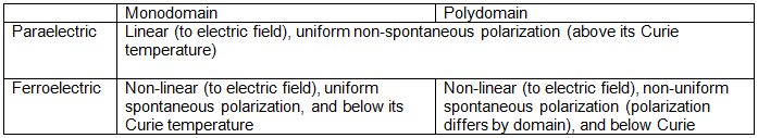
Dielectric materials are materials that can store and respond to electric charge but not conduct electricity. So they are an electrical insulator that can be polarized by an applied electric field. When they are placed in an electric field, positive charges are placed in the direction of the field, with negative charges in the opposite.
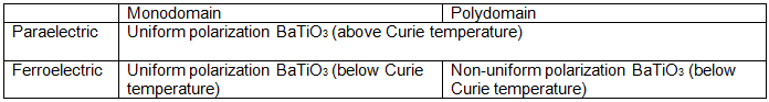
All materials that have a Curie temperature, are paraelectric when above their Curie temperature. However, not all materials have a Curie temperature, so you can still have paraelectric materials without a Curie temperature.
When a material is paraelectric, it becomes irrelevant whether a material is monodomain or polydomain, because the polarization are non-spontaneous.
Further example:
Applications:
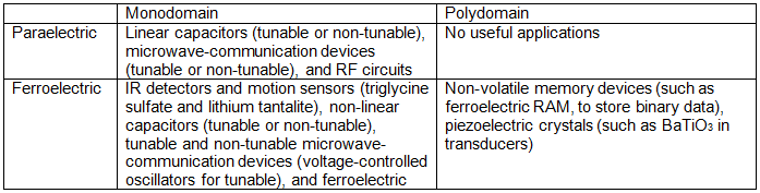
Note: a FeRAM uses a ferroelectric capacitor, where a thin ferroelectric material is sandwiched between 2 electrodes. Data is written by applying an electric field to polarize the material in 1 of 2 stable states (+ or – polarization). Data is read by measuring the polarization direction without destroying the state. FeRAM is faster than traditional non-volatile memories like EEPROM or flash because it doesn’t involve charge tunneling, and consumes less power than flash memory.
How can any material be used for devices, if being paraelectric requires it to be above its Curie temperature, meaning wouldn't it be really hot? And so, SrTiO3 has a Tc close to 0 K, while BaTiO3 has a Tc around 120 C, but in modified formulations (such as doping with other elements), the Tc can be shifted to meet specific application needs.
Fiber optics.
In 2022, about 21% of U.S. homes subscriber to fiber Internet, the 2nd largest. The largest is cable Internet, at 49%, then DSL at 3rd and 13%, then mobile wireless at 12%. About 43% of U.S. households have access to fiber Internet connection. The world's largest produced of optical fiber, as well as the largest manufacturer of fiber cable in North America, is Corning, with its manufacturing plant in North Carolina. Corning was most famous for making Gorilla Glass for the 1st iPhones in 2007.
Fiber-optic Internet is a type of broadband Internet, which the Federal Communications Commission defines as any Internet service which delivers download speeds of at least 25 megabits/second or upload speeds of at least 3 megabits/second. DSL (digital subscriber line) and cable delivers Internet over traditional copper telephone lines.
In fall of 1970, Corning came up with an optical fiber made of glass so pure that it allowed data to be sent over massive distances with minimal signal loss. Researchers Robert D. Maurer, Donald Keck, Peter C. Schultz, and Frank Zimar, had demonstrated an optical fiber with a low optical attenuation of 17 dB per km by doping silica glass with titanium. A few years later they produced a fiber with only 4 dB/km, using germanium oxide as the core dopant. Such low attenuations made fiber optics practical for telecommunications and networking. Corning became the world's leading manufacturer of optical fiber. In 1983, New York and Washington D.C. became the 1st cities in the world to be connected through a long-distance fiber-optic link, by Bell. The anatomy of a single optical fiber has a core made of ultra-pure glass being surrounded by a 2nd layer of glass, which reflects the light signal and traps it inside the core as it moves down the length of the fiber. Both layers of glass are then encased in a protective plastic coating.
In Q2 2022, Corning disclosed that the optical communications business was its largest segment by revenue, reaching sales of $1.3 billion, a 22% increase (followed by display technologies at $878 million, specialty materials at $485 million, environmental technologies at $356 million, and life sciences at $312 million).
Since 1970, Corning has made over 1.3 billion miles of optical fiber, from Concord, NC, and cable plant 70 miles northwest in Hickory, NC. Unlike traditional copper phone lines that transmit information as electrical signals, fiber optic cables are tiny bendable strands of glass where data is sent through as photons, lasers emitting pulses of light, at higher speed and using less energy. Moving photons is 5 to 20x less power use than moving electrons.
3 easy steps that Corning makes fiber is vapor deposition (use combustion to deposit glass soot on the outside of a rod), extreme heat (to purify the glass), then 3. stretch it to 125 microns.
Quasicrystals.
Quasicrystals are materials characterized by a quasiperiodic distribution of atoms arranged in a pattern violating the crystallographic symmetry rules that apply to ordinary (periodic) crystals.
Condensed matter physics.
Superconductors.
In a crystal, there are 2 main types of symmetries: point symmetries (or point groups) and space symmetries (or space groups). There are 32 crystallographic point groups, which include rotational, reflection, inversion, and rotoinversion symmetry. There are 230 unique 3-D space groups, which inlude translation symmetry, screw aces, and glide planes. This has to do with how superconductors are classified according to the symmetries of their gap function.
The symmetry of the underlying crystal lattice, described by its point group and space group, set the stage for what superconducting pairing symmetries are allowed. The gap function must transform according to 1 of the irreducible representations of the crystal's point group. In a crystal with a high degree of symmetry, the gap function might be an s-wave (fully symmetric) or take on a d-wave or p-wave characters that change sign or vanish along certain directions (nodal structures). These differences are dictates by the crystal's symmetry operations.
As superconductors, electrons form Cooper pairs. As each electron spin is 1/2, then when 2 electrons are paired, their total spin can be S = 0 (singlet, anti-parallel, anti-symmetric spin state), or S = 1 (triplet). Because triplet superconductors have symmetric spin wavefunctions, the spatial wavefunction must be antisymmetric, so both opposites for singlet superconductors.
Symmetry requirement: in the Pauli exclusion principle, for 2 electrons, total wavefunction = spin part * spatial part. As electrons are fermions, the total 2-electron wavefunction must be antisymmetric under exchange. When 2 electrons are swapped, total wavefunction = -total wavefunction.
The energy gap Δ(k), or the superconducting gap, describes the energy required to break a Cooper pair and create quasiparticles. It can depend on the direction of electron momentum on the Fermi surface. Nodes do not mean the Cooper pairs are permanently broken. They mean the pairing amplitude goes to 0 in certain directions, and quasiparticles can be excited with very little energy.
Conventional superconductors (where the gap is the same everywhere) typically have s-wave (isotropic) gap symmetry that remains the same in all directions, which is consistent with a fully symmetric pairing state.
Unconventional superconductor (the gap can vary with direction and may even go to 0 at certain points or lines), may have anisotropic gap functions such as d-wave (e.g., in high temperature cuprate superconductors), p-wave (as suggested in some heavy fermion or ruthenate superconductors), or other symmetries. These anisotropic gap functions often exhibit nodes (directions where the gap goes to 0), and their angular dependence directly reflects the symmetry of the crystal lattice.
A conventional superconductor has pairing explained by phonon-mediated pairing in BCS theory, while unconventional superconductor is pairing believed to come from non-phonon interactions (such as spin fluctuations, strong correlations), or where the order parameter has unusual symmetry. All s-wave conventional superconductors are singlet, but not all s-wave singlet superconductors are conventional.
Measuring the superconductor's heat transport are important to find details about the superconducting state, particularly the structure of the superconducting gap and the nature of the quasiparticle excitations. In superconductors with a full gap (s-wave), there are very few low-energy excitations at low temperatures, so the thermal conductivity is expontentially supressed. If the superconducting gap has nodes (as in many unconventional superconductors like d-wave or certain p-wave materials), there are low-energy quasiparticles available even at very low temperatures. Regarding symmetry information, measuring the how heat is conducted as a function of temperature (and sometimes direction), researchers can infer whether the gap is isotropic (uniform in all directions) or anisotropic (varies with direction), and whether it has nodes. This information is crucial for understanding the pairing mechanism that gives rise to superconductivity.
Pairing symmetries history: the 3 pairing symmetries were not discovered at th the the superconductors was discovered. The 1st superconductor to be discovered, mercury, in 1911, at Leiden Low Temperature Laboratory, was s-wave. The explanation didn't come until 1957 with BCS theory which showed superconductors like Hg have isotropic s-wave pairing. The 1st d-wave superconductor was YBa2Cu3O7, discovered in 1986 at IBM Zurich, but the d-wave symmetry wasn't confirmed until 1994-1995 through phase-sensitive Josephson experiments. The 1st p-wave superconductor was Sr2RuO4, strontium ruthenate, discovered in 1994 at Kyoto University. However, modern experiments after 2019 suggest the situation may be more complicated, and the exact pairing symmetry is still debated. However, before p-wave superconductors were proposed in solids, physicists already discovered p-wave pairing in superfluids, which was helium-3, in 1972, at Cornell University, which was the 1st experimental realization of p-wave triplet pairing.
| Orbital symmetry | Spin state | Orbital angular momentum | Pairing mechanism | s-wave | singlet | l = 0 | Conventional or unconventional |
| d-wave | most singlet | l = 2 | Unconventional |
| p-wave | triplet | l = 1 | Unconventional |
Qubits and fluxonium.
A qubit is a quantum system with a 2-dimensional Hilbert space. Therefore, in order to realize a qubit, all we need is a quantum system that has 2 possible states. Qubits can be generalized to a quantum system with a d-dimensional Hilbert space, which is called a qudit. Although qudits are being researched, qubits are the proposed building block of a quantum computer as they are analogous to classical bits in a classical computer.
A standard example of a qubit is the photon, wherein the photon's spin states form the computational basis. Recall that a photon, as a spin-1 particle, technically has 3 allowed spin states: l = 1 and m ∈ {-1, 0, 1} (where l is orbital angular momentum and m is magnetic angular momentum). However, relativistic quantum mechanics requires that the photon can only occupy the l = 1, m = ±1 states. Thus, we can label the m = 1 state as |1i and the m = -1 state as |0i, giving us a computational basis. Of course, 1 can also take the 2 spin states of a spin one half particle, such as an electron.
The qubit itself is a many-body system of interacting electrons designed and fabricated in the form of an electrical circuit, where quantized energy levels of a collective excitation mode are used as the bases for storing and manipulating quantum information. With the strong nonlinearity due to the Josephson effect and the large dipole moments that allow fast control and readout of the quantum states, superconducting qubits comprise versatile platforms for quantum information processing.
Fluxonium.
Fluxonium are a superconducting circuit of interest in modern research. The fluxonium qubit is a superconducting circuit in which a Josephson junction is placed in parallel with an inductor. Josephson junctions are formed by 2 superconducting electrodes separated by a thin, insulating barrier. The Josephson effect is when a voltage is applied across the junction, and Cooper pairs tunnel through the insulating material barrier, where the insulating material is surrounded by 2 superconducting wires and leading to a supercurrent without any voltage drop. The temperture of this has to be below 10 milliK. In quantum computing, chips that have qubits, also have resonators, composed of 2 lines of capacitors.
When a material becomes perfectly superconducting, its internal resistance is 0. Therefore, if a circuit’s material becomes perfectly superconducting, a given current in the circuit will never die, so superconducting circuits can be described in terms of quantum states. Therefore, physicists seek to realize qubits via superconducting circuit: they provide a long-lived quantum system from which we can form a computational basis.
Andreev reflection occurs at the inferface between a superconductor and a normal metal or semiconductor. When a electric impinges on the superconductor, it can be retro-reflected as a hole, forming a Cooper pair with an electron in the superconductor.
Superconducting qubits.
Superconducing qubits are an anharmonic LC circuit formed from a capacitor and a Josephson junction (or SQUID loop). Physically, superconducting qubits look like an RF circuit patterned in the superconductor film set on top of a Si or sapphire substrate or chip, typically accessed through an RF readout resonator. It can be 400 microns. Superconducting qubits are a promising avenue for low-threshold dark matter detectors via phonon sensing.
As of Jan. 2025, superconducting qubits have a gate-time of 100 nanoseconds (10-7), compared to superconducting ion trap have a gate-time of 100 microseconds (10-4). The gate-time of a qubit refers to the time it takes to peform a single quantum gate operation on the qubit, which is a key measure of the speed of quantum information procesing. Ion trap qubits used trapped ions (such as Ca+ and Yb+) manipulated with lasers or microwave fields to implement quantum gates.
SQUID.
A superconducting quantum interference device is a very sensitive magnetometer used to measure extremely weak magnetic fields, based on superconducting loops containing Josephson junctions. They are sensitive enough to measure fields as low as 5 * 10-18 T.
Plasmons.
Plasmons are 1 of the 6 types of quasiparticles: collective excitations of free electrons in a solid or liquid, typically occurring at the interface between a metal and a dielectric material or semiconductor. They are associated with the oscillations of the electron density in response to external stimuli, such as electromagnetic radiation. The word plasmon is due to gaseous plasma are a lot like metals, so let's use the word plasmon.
Can metals bonded to non-metals also be a plasmon? Yes, due to ligand-coats only interacting with the electrons, and the collective oscillations of the free electrons in the metal core. But it would not include compounds like KMnO44. The inability of KMnO4 to exhibit plasmonic behavior is more fundamentally related to its electronic structure and the absence of a free electron gas characteristic of metals. Compounds with d orbitals are a problem with plasmons.
Some semiconductors can be plasmons because they have high enough carrier density. In some cases, semiconductors with high carrier density, such as heavily doped semiconductors or those under intense optical excitation, can exhibit plasmon-like behavior. This behavior arises due to the collective motion of the excess carriers (electrons and holes) in response to an external stimulus, similar to the behavior of free electrons in metals. In such situations, the semiconductor behaves more like a degenerate electron gas, and plasmonic effects can be observed. However, the characteristics of these plasmons may differ from those in metals due to differences in carrier properties and band structure.
Magnons.
Within antiferromagnetic materials and metamaterials, magnons, with frequencies spanning tens of GHz to THz frequencies, exist at all wavenumbers. The availability of ultrafast magnons is largely responsible for the magnetism community’s recognition that antiferromagnets should play an active role in next generation electronics, magnetics, and opto-electronics. Some examples are antiferromagnetic based memories, spin-torque THz oscillators, and the usage of antiferromagnets as a building block for hybrid quantum systems.
Ferroelectric materials.
Ferroelectric materials can spontaneously polarize and stay polarized until they're exposed to an electric field. They also change shape in electric fields and can generate electricity under stress. Examples include lead titanate and tetragonal CH3NH3PbI3 (2017). In the early 2000s, if you went to the hospital to get an ultrasound, the system may take a whole room. Now, it's handheld.
News.
12/4/2023.
A group of physicists from the University of Washington and the U.S. Department of Energy (DOE) have seemingly discovered a new, controllable variation of superconductivity in an exotic, crystal-like material. Its superconductivity can be modulated according to the strain applied to it, to the point of turning it off at will. Simultaneously, they've apparently broken the record on how "hot" a field-effect superconductor can be before it loses its ability to conduct electricity, absent any resistance.
The research paper (published in Science Advances) describes a synthetic, crystal-like sandwich of both ferromagnetic (europium) and superconductive materials (iron arsenide), which showcase emergent superconductivity when placed in the proximity of a strong enough magnetic field. Doped EuFe2As2, as the material is called due to the addition of cobalt molecules to the synthesis process, takes advantage of europium's strong ferromagnetism, alternated with superconducting/nematic FeAs (iron arsenide) layers in a sandwich-like configuration.
The result is what's known as a field-tunable superconductor - 1 whose superconductivity features can be enabled through the application of external magnetic fields. In the case of doped EuFe2As2 (and by deploying specialized equipment alongside a combination of X-ray techniques), the research team showed how a properly aligned external magnetic field counterbalances the magnetic fields emanating from the ferromagnetic europium layers. This allows them to be reoriented - and once the originally chaotic magnetic fields are parallel to the superconducting ones, a zero-resistance state of matter emerges.
But doped EuFe2As2 has another secret: its superconducting capabilities can be turned off even in a strong enough magnetic field. All that's needed is to strain the material with a cryogenic strain cell - to apply pressure from a single side (uniaxially) with what's akin to an industrial, scientific-measurements-certified piston - to modulate how much resistance electrons find while traversing it. Under certain strain levels, the superconductivity of the synthetic material can be boosted enough so that an external magnetic field isn't required to enable a superconductive state. But after a point, not even pressure gets the engines going. 2 different mechanisms for superconductivity can only go so far, but they also open up several opportunities in customizing superconductivity - an additional lever to pull.
4/9/2026.
Governor Kathy Hochul today announced the beginning of installation of Tokyo Electron’s leading-edge 300 mm wafer coater/developer system designed to support the next generation of semiconductor manufacturing at NY Creates’ Albany NanoTech Complex. This tool, called the CLEAN TRACK™ LITHIUS Pro DICE™, applies and processes a light-sensitive layer on silicon wafers, which is the platform upon which computer chips are built. This allows researchers to fabricate the minute patterns needed for the next generation of advanced processors, memory, sensors and more. This is the 1st major piece of equipment to be delivered for the forthcoming High NA Extreme Ultraviolet (EUV) Lithography Center at Albany NanoTech, which will be North America’s 1st and only publicly owned, accessible High NA EUV Lithography research site.